T1#market
Google Reveals the TPU — Its Own Chip for Machine Learning
Metadata
- Date
- Decade
- 2010s
- Tier
- T1
- Sources
- 09
- Connections
- 05
- Tags
- #market
On Wednesday 18 May 2016, in his keynote at the Google I/O developer conference, CEO Sundar Pichai revealed a chip Google had kept secret: the Tensor Processing Unit (TPU), designed in-house for machine learning. "TPUs deliver an order of magnitude higher performance per watt than all commercially available GPUs and FPGA," Pichai said, as reported by PCWorld, and he added that the chips had powered AlphaGo, which had beaten Lee Sedol two months earlier.
It was an announcement, but not of a new product. A Google blog post published the same day said TPUs had been running inside its data centres for more than a year, and a paper the following year put their deployment at 2015. What Google revealed was a chip that had already been at work behind its search and maps services without anyone outside knowing.
The glossary entry for TPU defines the term and outlines later generations, and the entry for AI accelerators sets it beside GPUs, NPUs and ASICs. This page follows why Google built its own chip and how it came to be opened to others.
What Google disclosed
The blog post, by Google Fellow Norm Jouppi, made a few points briefly:
- The TPU is a custom ASIC built for machine learning and tailored to TensorFlow, Google's machine-learning framework
- Because machine learning tolerates reduced computational precision, the chip needs fewer transistors per operation and can fit more operations into the silicon
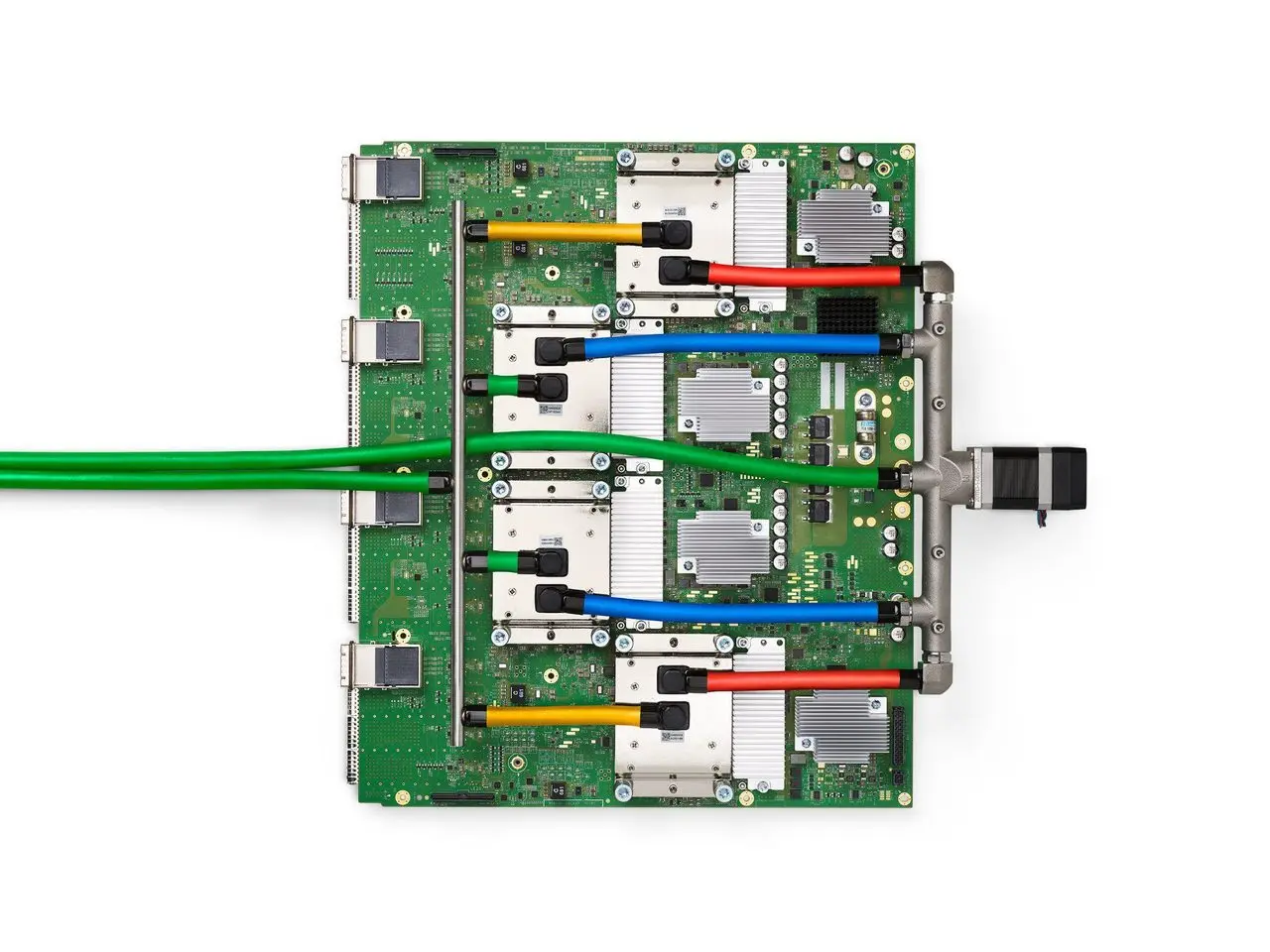
- A board carrying a TPU fits into a hard-disk slot in a data-centre rack
- From first tested silicon, the team had TPUs running applications at speed within 22 days
- TPUs already powered RankBrain, which improves the relevance of search results, and Street View
On performance, the post claimed an order of magnitude better-optimised performance per watt, "roughly equivalent to fast-forwarding technology about seven years into the future (three generations of Moore's Law)." It did not yet say what that was measured against. The analyst Patrick Moorhead, who attended I/O, told PCWorld the TPU was handling the running of trained models rather than the training itself. "It's not doing the teaching or learning," he said. "It's doing the production or playback." PCWorld also noted that SGI had sold a product called a Tensor Processing Unit in the early 2000s; Google said there was no connection.
Why Google built its own chip
The reasons came in a detailed post Google published a year later, in May 2017. Google had considered building an ASIC for neural networks as early as 2006, but the situation became urgent in 2013, when it realised that the fast-growing computational demands of neural networks could require it to double the number of data centres it operated.
ASIC development usually takes several years. Google designed, verified, built and deployed the TPU in 15 months. To get it into existing servers quickly, the processor was packaged as an external accelerator card that slots into a SATA hard-disk bay, connected to its host over PCIe Gen3 x16.
The numbers in the 2017 paper
In April 2017 Jouppi and 74 co-authors released a paper on the first-generation TPU, presented that June at ISCA, the International Symposium on Computer Architecture. What had been blog-post claims now came with figures.
| Item | First-generation TPU (per the 2017 paper and explainer) |
|---|---|
| Role | Neural-network inference only |
| Deployment | In Google's data centres since 2015 |
| Process, clock, power | 28 nm, 700 MHz, 40 W when running |
| Matrix unit | 65,536 8-bit multiply-accumulate units |
| Peak throughput | 92 TOPS |
| On-chip memory | 28 MiB, software-managed |
| Compared against | Intel Haswell CPU and NVIDIA K80 GPU in the same data centres |
| Average speed | About 15–30× the GPU or CPU |
| Performance per watt | About 30–80× higher |
The workload was production neural-network models representing 95% of the inference demand in Google's data centres. The paper also argued that the TPU's deterministic execution, without the caches, out-of-order execution and other features CPUs and GPUs use to raise average throughput, suited services that must meet 99th-percentile response-time targets. The multiples compare machines installed in the same data centres at the same time; against different hardware they would differ.
Training, then the outside world
The first generation did inference only; training still ran on GPUs and CPUs. That changed with the second generation, announced at Google I/O in May 2017.
Google said each new TPU device delivered up to 180 teraflops of floating-point performance and could both train and run models. Sixty-four of them, linked by a dedicated high-speed network into a "TPU pod", provided up to 11.5 petaflops. A large translation model that had taken a full day to train on 32 of the best commercially available GPUs now trained to the same accuracy in an afternoon on one eighth of a pod, Google said.
On 12 February 2018 Cloud TPU entered beta, letting outside developers rent TPUs on Google Cloud. Each board, built with four custom ASICs, offered up to 180 teraflops and 64 GB of high-bandwidth memory, at $6.50 per Cloud TPU per hour. Google said a single Cloud TPU could train ResNet-50 to the expected ImageNet accuracy in less than a day for well under $200. A chip built for Google's own services had become a cloud product.
| Date | Event |
|---|---|
| 2006 | Google considers a neural-network ASIC (company account) |
| 2013 | Surging compute demand makes it urgent |
| 2015 | First-generation TPUs running in data centres |
| March 2016 | AlphaGo plays Lee Sedol, running on TPUs |
| 18 May 2016 | TPU revealed at Google I/O |
| April 2017 | First-generation paper released (presented at ISCA in June) |
| May 2017 | Second generation, with training and TPU pods |
| 12 Feb 2018 | Cloud TPU beta opens |
| April 2025 | Seventh-generation Ironwood announced |
| 23 Oct 2025 | Anthropic announces plans to use up to a million TPUs |
The TPU a decade on
Nine years after the reveal, at Google Cloud Next 25 in April 2025, Google introduced the seventh-generation Ironwood, which it called its first TPU designed specifically for inference. Up to 9,216 liquid-cooled chips can be joined into one pod, which Google put at 42.5 exaflops. Each chip has 192 GB of high-bandwidth memory, and Google says Ironwood is nearly 30 times more power-efficient than its first Cloud TPU of 2018. These are all Google's own figures.
On 23 October that year Anthropic announced it would expand its use of Google Cloud, including up to one million TPUs, in a deal it said was worth tens of billions of dollars and expected to bring well over a gigawatt of capacity online in 2026. A chip built so that Google would not have to double its data centres had become one of the ways other AI companies secured compute.
What changed
The TPU's reveal was the moment one of the largest cloud operators showed, with working silicon, that AI compute did not have to mean GPUs. As training on general-purpose GPUs with the CUDA software stack spread (see the release of CUDA), Google took the other road, narrowing the circuitry to its own workloads, and then published how it had done so. From the late 2010s GPUs, too, began devoting dedicated hardware to low-precision matrix arithmetic (see the launch of NVIDIA Blackwell, which added a 4-bit format).
See also the hardware timeline.
Questions this page answers
- When did Google announce the TPU?
- CEO Sundar Pichai revealed it in his Google I/O keynote on 18 May 2016. By Google's account TPUs had by then been running in its data centres for more than a year; the 2017 paper says they had been deployed since 2015.
- How did the first TPU differ from a GPU?
- The first generation was an ASIC for neural-network inference only, built around a matrix unit of 65,536 8-bit multiply-accumulate units. In its 2017 paper Google reported it was on average 15 to 30 times faster than the Intel Haswell CPU and NVIDIA K80 GPU in the same data centres, with 30 to 80 times higher performance per watt.
- Can anyone outside Google use a TPU?
- Yes. Cloud TPU entered beta on 12 February 2018, letting developers rent TPUs by the hour on Google Cloud, at $6.50 per Cloud TPU per hour at the time.
Sources
Pichai's statement at I/O, AlphaGo, no link to SGI's product of the same name, Patrick Moorhead's view
PrimaryAn in-depth look at Google's first Tensor Processing Unit (TPU) — Google Cloud Blog, May 12, 2017
Consideration in 2006, urgency in 2013, deployment in 15 months, 28 nm / 700 MHz / 40 W, a card that fits a hard-disk slot
Last updated: